
Introduction to Flash Memory Technology
Flash memory, a form of non-volatile storage, has become an indispensable component in modern electronic devices. It is widely used in smartphones, tablets, digital cameras, USB drives, solid-state drives (SSDs), and numerous embedded systems due to its unique combination of durability, speed, and energy efficiency. This article aims to unlock the fundamentals of NAND flash memory, one of the two primary types of flash memory technology, and provide a comprehensive understanding of its architecture, operation principles, and applications.

NAND Flash Memory Architecture
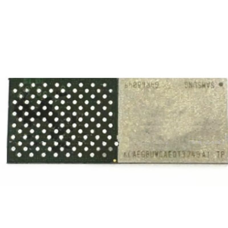
At the heart of NAND flash memory lies its namesake structure: the NAND gate. A NAND gate is an elementary logic circuit that produces a high output only when all its inputs are low; otherwise, it outputs a low signal. In NAND flash memory, multiple transistors are interconnected in series to form a NAND cell array, resembling the arrangement of a NAND gate. Each cell stores a single bit of data by controlling the electrical charge stored in a floating-gate transistor.
Floating-Gate Transistor
The floating-gate transistor is the fundamental building block of NAND flash memory cells. It consists of a control gate, a floating gate, and a channel sandwiched between two source and drain regions. The floating gate is electrically isolated, allowing it to retain a charge even when power is removed. When a voltage is applied to the control gate, electrons can tunnel through a thin oxide layer and either accumulate on the floating gate (programming, representing a logical ‘0’) or be removed from it (erasing, representing a logical ‘1’). This charge storage mechanism enables non-volatile data retention without continuous power supply.
Cell Array Organization
NAND flash memory arrays are organized in a matrix structure, with rows (wordlines) connected to the control gates of each cell in a row and columns (bitlines) connected to the source and drain regions of each cell in a column. To read, program, or erase data, the appropriate wordline and bitline are activated, enabling precise control over individual cells or groups of cells. The cells are further grouped into blocks, which are the smallest erasable units in NAND flash memory. Blocks typically contain thousands to millions of cells and are arranged into planes, enhancing parallelism and overall performance.
Operation Principles of NAND Flash Memory
Understanding the operational aspects of NAND flash memory is crucial for appreciating its capabilities and limitations. Key operations include reading, programming (writing), and erasing data, as well as error correction and wear leveling.
Reading Data
Reading data from a NAND flash cell involves applying a specific voltage to the control gate. If the floating gate contains a charge (programmed state), the threshold voltage of the transistor will be higher, resulting in a lower current flow through the channel when the bitline is biased. Conversely, if the floating gate is depleted of charge (erased state), the threshold voltage will be lower, allowing a higher current flow. By comparing the sensed current with a reference level, the memory controller can determine whether the cell stores a ‘0’ or ‘1’.
Programming Data
Programming a NAND flash cell entails injecting electrons onto the floating gate. This is achieved by applying a high voltage to the control gate while the bitline is grounded, creating an electric field that facilitates electron tunneling from the channel to the floating gate. The process is inherently slower than reading due to the need for precise control over the amount of charge injected to ensure reliable data storage and distinguish between programmed states.
Erasing Data
Erasing a NAND flash block involves removing the charge from all cells within the block simultaneously. An erase voltage is applied to the p-well (substrate) while the control gates are grounded, causing electrons to tunnel out of the floating gates and back into the substrate. Erasing is faster than programming since it operates on a block level rather than individual cells, but it also introduces challenges related to data management and wear leveling.

Error Correction and Wear Leveling
Due to the inherent limitations of the floating-gate transistor and the manufacturing process, NAND flash memory is prone to errors and data retention issues over time. Error correction codes (ECCs) are employed to detect and correct these errors, ensuring data integrity. Wear leveling algorithms, on the other hand, evenly distribute write and erase operations across the entire memory to mitigate the effects of cell wear and prolong the lifespan of the device.
Applications and Evolution of NAND Flash Memory
NAND flash memory’s versatility and performance have made it the go-to storage solution for a wide range of applications, driving advancements and diversification within the technology.
Consumer Electronics and Enterprise Storage
In consumer electronics, NAND flash memory powers the storage subsystems of smartphones, tablets, digital cameras, and USB drives, providing fast access to data and enhanced user experience. In enterprise settings, SSDs based on NAND flash offer substantial improvements in input/output (I/O) performance, energy efficiency, and reliability compared to traditional hard disk drives (HDDs), transforming data center architectures and enabling new computing paradigms like cloud computing and big data analytics.
3D NAND and Emerging Technologies
To address the ever-increasing demand for higher storage capacities and better performance, NAND flash technology has undergone significant evolution. One major breakthrough is the introduction of 3D NAND, which stacks multiple layers of cell arrays vertically, dramatically increasing storage density while maintaining or improving performance. Other emerging technologies, such as Resistive RAM (ReRAM) and Phase Change Memory (PCM), aim to challenge NAND flash’s dominance by offering even greater scalability, endurance, and energy efficiency.
Conclusion of NAND flash memory technology
In conclusion, NAND flash memory technology, with its unique architecture and operation principles, has revolutionized the storage landscape. Its ability to store data reliably without a constant power supply, combined with its high performance and compact form factor, has made it indispensable in today’s digital age. As advancements like 3D NAND and novel non-volatile memory technologies continue to push the boundaries of what is possible, NAND flash remains at the forefront of storage innovation, shaping the future of consumer electronics, enterprise storage, and beyond.